|
Scios 2 Dualbeam FIB-SEM
|
|

|
| |
The W.M. Keck Center for Nanoscale Optofluidics has a dedicated nanofabrication facility in 268 Baskin Engineering that houses our Thermo Scientific Scios 2 Dualbeam microscope, a versatile, high-resolution, low-vacuum SEM/FIB for 2D and 3D material characterization and analysis.
Innovative electron and ion optics combined with a unique environmental SEM operating mode will expand your laboratory’s capabilities, providing better, faster and more comprehensive materials characterization, analysis and sample preparation.
Our staff scientist, Dr. Tom Yuzvinsky, is on hand to assist with imaging, interpretation, and experiment design. He will also train students who wish to use the microscope independently (i.e. after hours or during other low-use periods).
|
|
|
Recharge Rates:
| |
| |
SEM
|
FIB
|
|
Internal Users:
|
$35/hour
|
$50/hour
|
|
External Users:
|
$180/hour
|
$190/hour
|
|
Contact: Dr. Tom Yuzvinsky, yuzvinsky-at-soe.ucsc.edu
|
|
|
|
| |
| Imaging |
| |
|
|
|
|
|
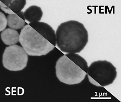
Transmission microscopy using our STEM detector can provide simultaneous surface imaging and sample density characterization.
|
|
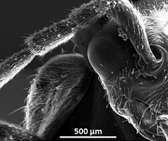
Biological samples can be sputter coated with gold or imaged directly with our environmental mode.
|
Available Imaging Modes:
| |
Primary Applications
|
Compatible Samples
|
|
Secondary electron detection (standard SEM)
|
Nano- or micro-scale inspection
|
Dry, conductive samples (insulating samples can be sputter coated)
|
|
Scanning transmission electron microscopy (STEM)
|
Highest resolution inspection and relative density characterization
|
Nanoparticles on TEM grids, very thin cross-sections
|
|
Environmental / low vac mode
|
Inspection of wet or insulating samples
|
Any sample suitable for low vacuum
|
|
Focused ion beam (FIB) imaging
|
Visualization of metal grains
|
Dry, conductive samples
|
|
| |
|
Fabrication and Modification
|
| |
|
|
| |
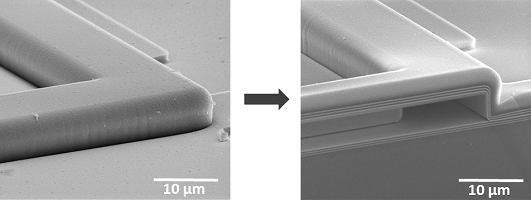
Samples can be cross-sectioned in situ with the ion beam for subsurface imaging and characterization.
|
|
|
|
|
|
|
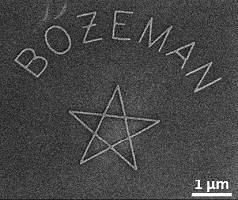
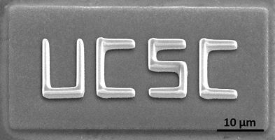
Our microscope is equipped with NPGS and a high speed beam blanker for high resolution electron beam lithography.
|
Platinum, tungsten, and/or silicon oxide can be locally patterned using ion or electron beam induced deposition.
|
| |
Available Fabrication/Modification Modes:
| |
Primary Applications
|
Compatible Samples
|
|
High current ion milling
|
In situ cross-sectioning, large area material removal
|
Dry, conductive samples
|
|
Low current ion milling
|
Nanopore fabrication, nanoscale material removal
|
Dry, conductive samples
|
|
Ion- or electron beam deposition
|
Direct deposition of Pt or SiO2
|
Dry, conductive samples
|
|
Electron beam lithography
|
Pattern writing for subsequent metal deposition or etching
|
Flat, resist-coated samples
|
|
| |
|
Outreach
|
| |
|

|
| |
In addition to research use, we invite users from the UCSC community and beyond to take advantage of our system for instructional and outreach purposes. Come show your students how fascinating the world can be at the microscale!
|
|
|
| |
|
For more information or to schedule a session, please email our staff scientist,
Dr. Tom Yuzvinsky, at yuzvinsky-at-soe.ucsc.edu
|